Joel Slaby

Joel Slaby

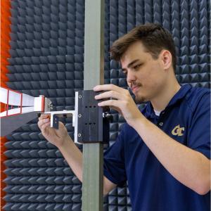
Some might say I grew up in the windy city, Chicago, braving the bitterly cold winters. Others may say the cornfields of southern Indiana or even Pittsburgh, the City of Bridges. I’ve spent enough time in all of these places to form incredible memories and deep connections, but the truth is Atlanta has become my home for more than six years.

I’m Joel, a 3rd-year electrical engineering graduate student in Dr. Stephen Ralph’s Lab with a particular research interest in integrated silicon photonics (SiP). I joined Georgia Tech for my undergrad and immediately jumped into the community. I started in a living-learning community, Grand Challenges, where we focused on working towards solutions to the “14 Grand Challenges for Engineering in the 21st Century.” These were lofty goals for naive freshmen, and yet the community created a critical environment for cultivating new ideas and fostering action toward those ideas. I also participated in EcoCar, a competition to convert a real gas car to a hybrid. These projects sparked my drive to directly engage with industry and convert the technical knowledge from engineering classes to tangible technological developments. As far as I knew, I was set on graduating and going straight to industry.

However, I refused to end my undergrad career without a taste of research and thus joined Dr. Ralph’s lab during my final year after thoroughly enjoying one of his classes. Here I was immediately placed on a project to develop new silicon photonic designs using density-based topology optimization, a design method my colleague and mentor, Dr. Alec Hammond, pioneered here at Tech. This project was practical, the designs are fabricated at commercial foundries, cutting edge, current state-of-the-art design methodology, and impactful, active interest by universities and companies globally for developments in this field. Needless to say, I was hooked, and decided to stay for my master’s and shortly after, my PhD.

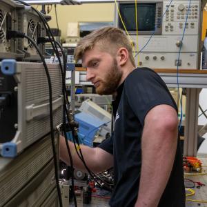
I love to move around and experience new places. I believe it keeps the world fresh and encourages a diversity of mind. But I decided to stay at Georgia Tech and pursue my Ph.D. because of this lab and this research. My primary research goal is to continue the advancement of integrated silicon photonics from a lab experiment to commercial solutions. SiP generally stated, is the transition of optical systems from large discrete components to small integrated silicon chips. This technology benefits from widespread integration by taking advantage of standard silicon CMOS processes used for electronics. Improvements in SiP directly affect data centers, satellite technology, virtual reality, high-performance computing, and more. To that end, I deliver on a number of research projects including the design and characterization of SiP systems for harsh environments such as aerospace through an NSF project called EPICA. I also work on developing a repeatable, commercially viable, and open-source fiber attach process through a collaborative project with DARPA and industry partners (KANAGAWA). As SiP continues to advance, this research is critical to ensure its success and widespread adoption.

Finally, unlike what most people believe, it’s not all work and no fun in graduate school. One of my favorite hobbies is crafting escape room puzzles. Every now and then, often for special occasions like birthdays or graduations, I present a series of connected challenges to unsuspecting friends. These puzzles have previously included bar crawls with sequential challenges revealing the location of the next bar, or group challenges where individuals were separated and had to use walkie-talkies to communicate and solve the puzzles. So, whether you meet me in the lab or somewhere else, be prepared for a puzzle.

“You know you’re in the right place when at least once a week you think to yourself, ‘I can’t believe I get paid to do this’ and in the same week ‘I’m not paid enough for this’” — Dr. Stephen Ralph
Joel
Slaby
Show Regular Profile

Seung Yoon Lee

Seung Yoon Lee

What is your background?

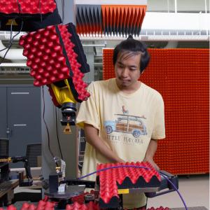
Seung Yoon Lee is a Ph.D. student in the School of Electrical and Computer Engineering at Georgia Tech, working in the mmWave Antennas and Arrays Laboratory supervised by Prof. Nima Ghalichechian. He received his B.S. in computer and communication engineering from Korea University, Seoul, South Korea, in 2016, and his M.S. in electrical engineering from the Pohang University of Science and Technology (POSTECH), Pohang, South Korea, in 2018. Prior to Georgia Tech, he worked at Samsung Research and SK Hynix for four years.

Prior academic/industry experience

Seung Yoon Lee completed his master's degree at POSTECH under Prof. Wonbin Hong, introducing the world's first Antenna-on-Display (AoD) concept for mmWave 5G communication. Afterwards, he was required to complete mandatory military service. He was given the opportunity to fulfill this obligation through alternative service by doing several years of research at a top-tier R&D company in Korea. Accordingly, he joined SK Hynix, where he performed numerous cutting-edge SPICE memory model extraction and developed on-chip inductors for high-speed memory products. Later, at Samsung Research, he designed a mmWave Reconfigurable Intelligent Surface (RIS) for next-generation 5G communication technologies.

Why Ph.D.?

During my master's program and subsequent 4 years of industry research, I discovered a passion for identifying and solving problems related to RF, antennas, and metamaterials.  Additionally, I was motivated to collaborate with top students in the USA, which led me to leave my previous position at Samsung, despite its positive culture and salary, to pursue a Ph.D. I am in my second year of mentoring undergraduate students at Georgia Tech, driven by a passion for sharing experiences and guiding future engineers. After graduation, I aim to propose and solve intriguing RF-related topics in academia, or in industry, and contribute to cutting-edge research aligned with a company's development direction.

Why Georgia Tech?

I chose Georgia Tech primarily because of my interview with Dr. Nima Ghalichechian, my current advisor, and his expertise in mmWave antenna arrays, aligning with my research interests. I was drawn to Dr. Ghalichechian ‘s lab because their approach of fabricating test samples in-house appealed to me, offering an opportunity to enhance my microfabrication knowledge. Additionally, I aimed to take classes from distinguished professors in my research area, electromagnetics, and collaborate with renowned professors in nanophotonics and electronics. The presence of the Marcus cleanroom, facilitating my microfabrication work, was also a factor in my decision.

Research you’re working on currently & what impact do you believe it will have

The International Telecommunication Union (ITU) predicts global mobile video traffic will account for more than 75% of total mobile traffic by 2030, which is due to the appearance of data-intensive applications such as virtual reality, augmented reality, and high-fidelity mobile holograms. In order to prepare for the potential huge increases in throughput, research on antennas operating at mmWave (30-300 GHz) band communications is being actively conducted which is thanks to its wide range of channel bandwidths available compared to the conventional microwave (i.e. < 3 GHz) band.

I aim to develop a highly efficient electronically scanned on-chip antenna array operating in the mmWave band, incorporating low-loss vanadium dioxide switches through monolithic integration. The objective is to design, fabricate, and characterize a V-band on-chip electronically scanned array for mmWave high data-speed wireless systems. This approach addresses the fundamental challenge of conventional low-efficient on-chip antenna arrays for next-generation 5G and 6G communications.

Tell us about anything else you wish to share like a personal hobby or talent 

To manage stress, I watch MLB or other sports games and play soccer on special occasions. I enjoy exploring new places in the United States that I've not been to, such as New York, Miami, and San Francisco.

Seung Yoon
Lee
Show Regular Profile

Mozhgan Hosseinzadeh

Mozhgan Hosseinzadeh

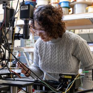
I discovered the major I was passionate about when I was accepted into the national physics Olympiad, prompting me to delve into subjects with greater depth. For my undergraduate studies, I pursued electrical engineering, with a primary academic focus on wireless communication Circuits. Opting to pursue graduate studies at Georgia Tech, I believed it was the place where I could push beyond my limits and embrace challenges. My research at Tech had a major turn and now my pursuit involves enabling Silicon photonics for space optical communications. I believe my research has the potential to revolutionize communication technologies in space and expand our comprehension of the underlying principles as well as a promise for practical and innovative applications in the commercial realm. Outside the lab, I enjoy going on hikes, practicing guitar lessons, or exploring the city.

Mozhgan
Hosseinzadeh
Show Regular Profile

Walter Disharoon

Walter Disharoon

What is your background?

I am a Ph.D. Student working in the mmWave Antennas and Arrays Lab advised by Prof. Nima Ghalichechian. I received my B.S. in Electrical Engineering from Kennesaw State University (KSU) in 2021 and recently completed my M.S. at Georgia Tech (GT) in Spring 2023. My background prior to Tech was in RF systems, RF FPGAs, and antennas. In my time at GT, I have received an ECE Freshmen Fellowship, a fellowship from Qualcomm, and the Georgia Tech Research Institute (GTRI) Graduate Student Fellowship. As part of the GTRI Fellowship, I am co-advised by GTRI faculty member Dr. Joshua Kovitz.

 Undergrad experience

There were a few key experiences at KSU that built the person I am. Prior to becoming interested in RF and research I spent time as a supplemental instruction leader (SIL) for chemistry and physics. SILs are students who did well in historically difficult courses who return to help other students succeed. I spent two years being an SIL, where I gained appreciation and passion for helping students grasp new concepts. I learned many skills through being an SIL in making learning interesting and how to ignite a stronger passion in the students, which helped with my experience as a graduate teaching assistant at GT. Later, I went searching for internships, which landed me at GTRI for a Co-Op, where I had the pleasure of working in the Sensors and Electromagnetic Applications Lab as an RF engineering student assistant. I enjoyed this experience as it taught me many of the valuable skills and intuition that I still use to this day when designing antennas and other RF systems.

 Why grad school?

During my time at GTRI, I noticed that a lot of the work that I found to be interesting was being led by engineers with master’s and doctoral degrees. My goal is to work on cutting edge research in a top-level research team in antenna or RF system design such as those at Qorvo, Qualcomm, Apple, etc. I chose particularly to pursue a Ph.D. to gain valuable experience working with experts in antenna design, fabrication, and testing. Furthermore, when I was an SIL, I came to enjoy the process of helping students learn new concepts and raising their interest in subjects I enjoy, so the Ph.D. is a natural progression towards being able to teach in the future if I return to academia after my future work in the industry.

 Why Georgia Tech?

I had three main reasons for choosing GT: The professors, reputation, and location. In my time at GTRI, I only heard positive things about the faculty at GT particularly in the electromagnetics department, which I can only agree with after having taken classes with many of the faculty here. Second, GT has a reputation for not only electromagnetic design, but also the fabrication and testing with state-of-the-art facilities such as the IEN cleanroom. Finally, the location of GT was convenient for staying close to friends and family. I was particularly drawn to Dr. Nima’s mmWave Antennas and Arrays Lab due to their interesting work in phase change material (PCM) devices.

 Research you’re working on currently and what impact do you believe it will have.

I am working on PCM enabled reconfigurable surfaces, particularly a reconfigurable reflectarray and a spatial limiter. In the reflectarray, we leverage the sharp nonlinearity of vanadium dioxide films to manipulate the electromagnetic waves polarization or direction, which could revolutionize systems for 5G and beyond communications. The spatial limiter takes advantage of nonlinearity to protect sensitive electronics from malicious or unintentional interference sources.

Tell us about anything else you wish to share like a personal hobby or talent.

I have been enjoying the pickup soccer put on by the ECE department and recently I have re-picked up rock climbing which both have been a great way to stay active and reduce stress.

Walter
Disharoon
Show Regular Profile